“Standard Processes Are of No Use to Us in European Semiconductor Manufacturing”
Why does the semiconductor market play such an important role?
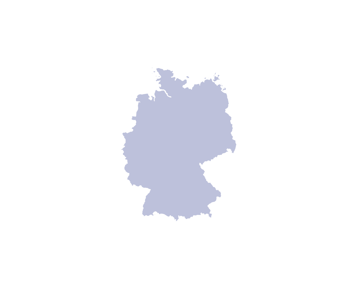
Dana Nikolaj: Semiconductors are simply everywhere. They are the heart of a chip or microchip and thus the central building block of all electronic components and thus of all digital devices. The automotive industry’s transformation towards electric vehicles, the steadily increasing electrification and continuously rising demand for communication technologies require ever smaller and more powerful chips. The traditional semiconductor market is clearly in Asia. However: In recent years, the need for a sustainable and resilient supply chain has become increasingly important. Therefore, Germany and the European Union have made it their mission to build and promote a chip ecosystem in Europe. The ambitious goal is to increase semiconductor manufacturing in Europe from the current 10% to 20% of the total global market by 2030.
Two years ago, non-deliverable chips were primarily a problem for the automotive industry. How do you see the “hunger for chips” with regard to the breakthrough of artificial intelligence?
The 2020/2021 chip crisis has fueled decisions for a more independent supply chain and thus for further investments in technology within Europe. The demand for constant automation, improved and ubiquitous artificial intelligence and, above all, energy efficiency and sustainability is becoming increasingly urgent – semiconductors are the basis for all these topics. And here, of course, we also see great opportunities for us.
What experience does Leadec have in the semiconductor field?
The first order came a few years ago for the intralogistics planning in a new wafer plant in Dresden. At that time, it was a jump in at the deep end for us. But together with the customer, we succeeded in developing and implementing the right intralogistics for handling highly sensitive raw materials for semiconductor production. The experience we gained there then served as a reference for subsequent projects, so that we are now active in other production facilities of well-known manufacturers. Be it maintenance, logistics and project-specific automation solutions for utility supply or test stands.
How are chip plants different from other production facilities, for example for vehicles?
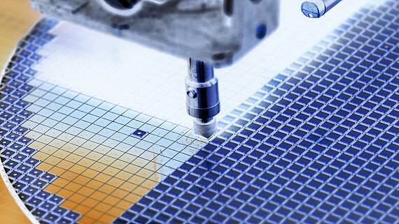
We are dealing with high-quality and at the same time particularly sensitive goods. The manufacturing environment of semiconductors, chips and other electronic components is highly automated and subject to very special requirements, e.g., with regard to room air, cleaning or shock sensitivity. For example, even a tiny dust particle falling on the surface of a semiconductor wafer can contaminate it in such a way that a whole series of electrical components becomes unusable. That’s why you see few people in traditional wafer fabrication facilities and cleanrooms, and little action compared to a traditional production facility. Much happens inside the equipment or is not visible to the eye.
What does this mean for the Leadec specialists working at the plant?
Our employees are aware that they are dealing with products that have to meet the highest requirements in terms of safety, handling and traceability. That brings with it a lot of responsibility. If, for example, something happens during the acceptance of goods for a component that has a production time of three years, then this has far-reaching consequences. In addition to basic skills, further education and training are therefore necessary in order to gain access to the individual production areas at all. The regulations are extremely strict, and we are familiar with them.
What are the greatest opportunities for Leadec as a service specialist in the semiconductor industry?
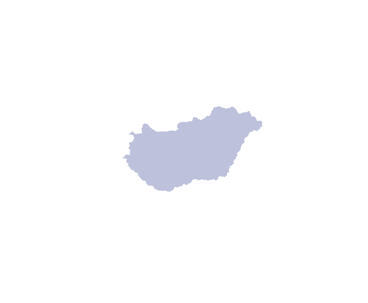
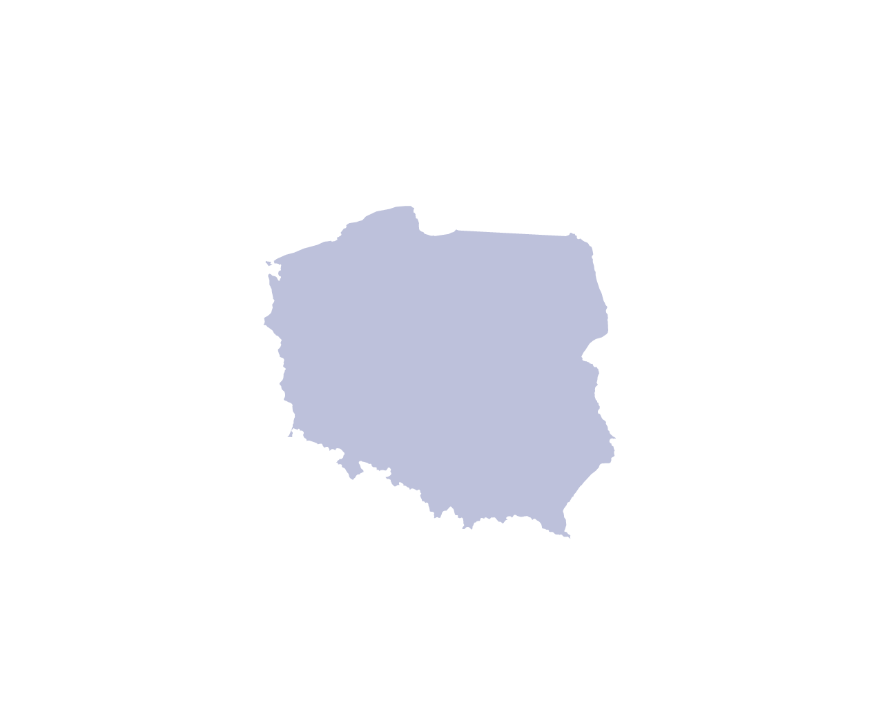
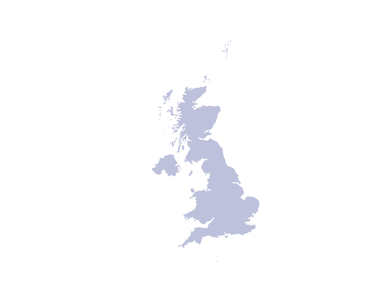
The biggest opportunities lie in the newly planned investments through the European Chip Act. The global market leaders such as Infineon, Intel and Globalfoundries are investing not only in Germany, but also in Austria, Poland, and the UK – these are precisely the regions where we have a strong footprint. The new construction and expansion of production facilities, the so-called “fabs,” offer us the opportunity to jointly design the outsourcing of ancillary processes with the customer at an early stage. Here we can offer solutions ranging from automation technology to operations. It is a real competitive advantage that we bring a lot of experience to support this greenfield approach, where a completely new production facility is built on a previously unused or “greenfield” site.
One thing is clear: in Europe, everyone, customers as well as suppliers and service providers, has to deal with the same challenges. It’s a new field. And in semiconductor manufacturing in Europe, standard processes are of no use to us. Instead, we have to be flexible, continuously learn and become pioneers. The time is right.

